T3 Rise of the machines

Evolution
Version 0
For version zero of the tracker I tried using off the shelf 'personal tracking' devices, this proved that it was possible to build my own tracking site. Initially I thought I really didn't want to spend any time trying to build my own device, but inevitably concluded that was the solution.Version 1
The first incarnation of the custom tracker was the klutzy A9G based system - well it wasn't klutzy at first, but after several iterations and enhancements it ended up that way. The A9G was incredibly cheap and worked reasonably well, but the module has some major design flaws and it can't do bluetooth (hence the klutzing).Version 2
The second version switched to using the RAK5010 based board, again it started elegant and ended up with multiple improvements. This definitely showed the type of hardware I wanted to use, this was an excellent combination of superb mobile/GPS device - the BG96, with a really good processor module - the NRF52840. Initially I decided I definitely didn't want to build something like this myself.... but inevitably...Version 3
So the plan now was to design and build a custom board incorporating all the improvements and ideas that I'd had working with the v2 design, since I've been impressed and happy with the RAK hardware with its use of the BG96 combined mobile and GPS module, my design is basically equivalent, although I'm using a Holyiot 18010 module for the processor to save the bother of having to build the Bluetooth and clock connections. The main improvements are to build in a decent battery monitor (MAX17048), better charger and power converters to provide 3.3v I/O and I2C interfaces. Plus other minor basic improvements such as add 'a power switch', better I/O ports, programming socket and so on.
This is pretty much the most complex project design and build I've done so far, my first proper surface mount project built onto a four layer circuit board that includes both large LGA chip modules (100+ pins) and absolutely 'tiny' LGA modules - 2.5mm x 1mm with 10 pads, spaced 0.15mm apart. Also the layout needs careful attention for the antenna traces and data lines.
Surface mounting
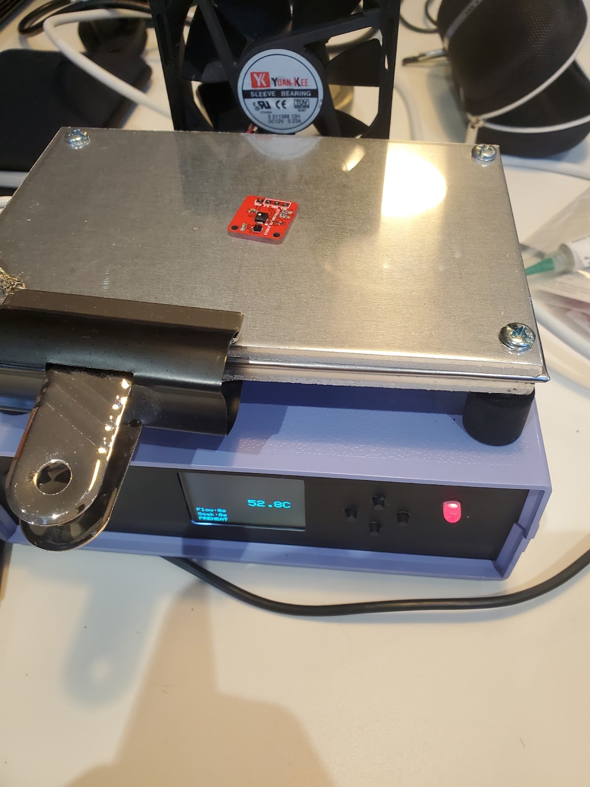
The first hurdle and "initial pre-project project" was learning how to make surface mount boards, I'd managed to avoid them all my life and only ever used through hole components before, so project #1 was constructing a home make SMD hotpate.
I hashed together an initial working device from an old power supply, raspberry PI and "bits"
 |
| Initial hacky hotplate. |
It worked and I used it to desolder some boards to test out the idea, concept, setup and so on and work out what I wanted in a finished setup, the first decision was a raspberry pi is definitely not the appropriate controller. So it was time to progress to a decent "compact" all in one setup, preferably with a micro-controller to be "turn-key".
After a few different designs, heating plates and cases... I settled on an Arduino micro driven device with a home-made mica heater platform:
 |
| Hotplate innards. |
The final build was a nice compact, self-contained unit. At the moment the fan hangs off the back so that could do with being moved to underneath the plate, but it does the job.
 |
| Working hotplate |
Ignore the dog-clip, that was a temporary necessity!
The first test run building some small CO2 sensors (another project to write up sometime) was a great success, although the software running the heater ended up being really primitive, it would be nice to spend some time to make it a bit slicker and smarter.
There's a "heat profile" to follow for different solders and devices, but I ended up just working out the heating times and just hardcoding a routine to adjust the heater for set periods of time.
 |
| A reflow heat profile |
I'd like to write a smarter adjustable heat controller program for it, I tried a couple of existing projects using PID logic, but none worked as well as my manual routine.
KiCad designing
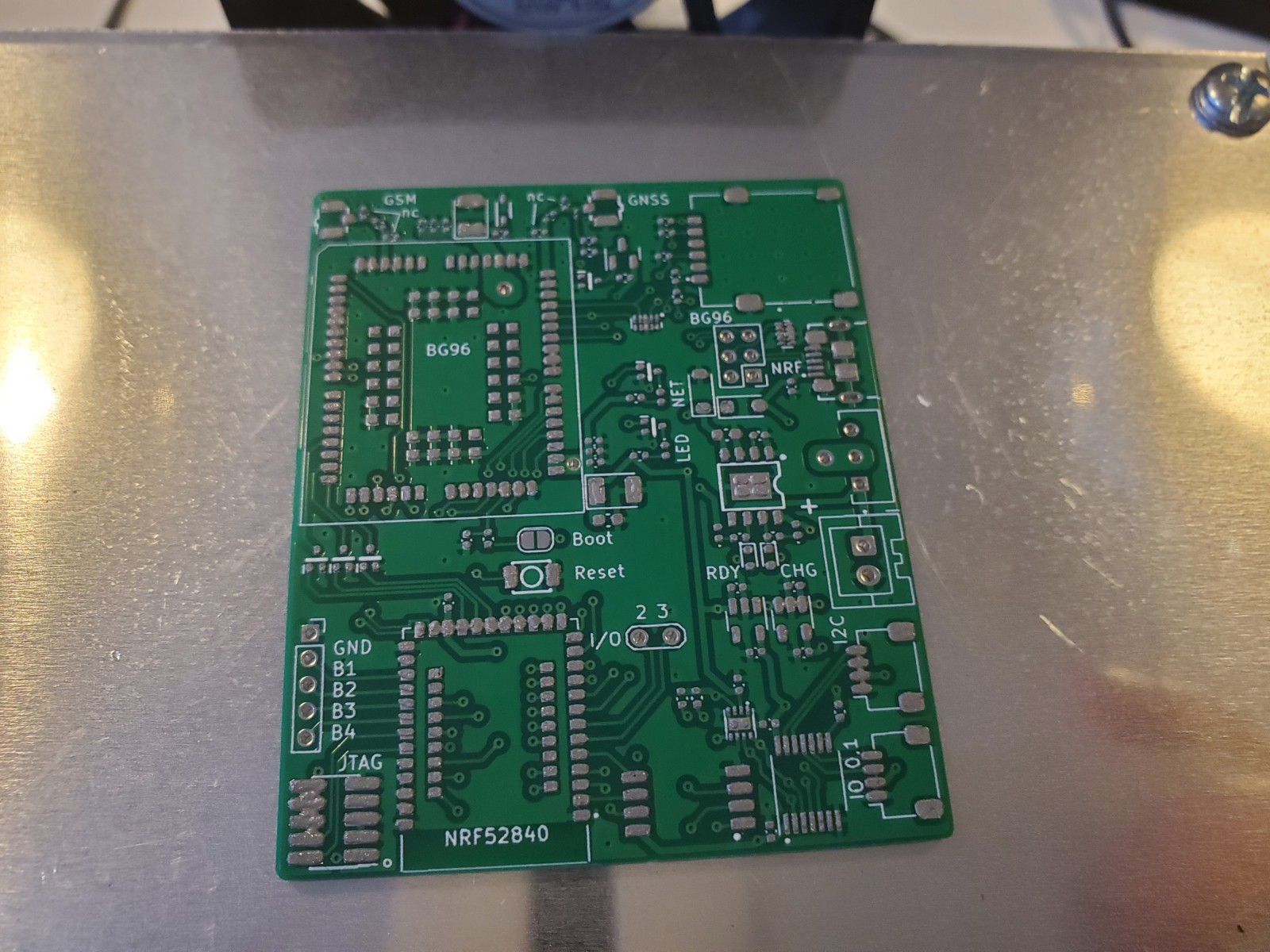
After several weeks of designing and planning, and learning KiCad the PCB design software. I had a good design and sent off for a board to be made. I designed a four layer board, although with components only on one side to make it easier (actually manageable) to solder. (quick aside - it's just incredible what technology is available to hobbyists now!)
 |
| 3D render of first design |
A few weeks later (I went for the budget service) the first board arrived back. It was so exciting to see in the flesh, although I wasn't ready to start building yet and I didn't have all the parts yet (a separate story).
 |
| The first board back with metal stencil |
 |
| Solder paste jig |
With the metal stencil for the solder I did a test run to practice my application technique and see how/if the hotplate melted the solder. Did it look ok?
 |
| Solder paste applied |
 |
| Solder paste melted |
Yes, the solder looks superb... just need the components on next time. 😄
Redesign
A great first success! In the meantime I'd re-read the hardware design notes and decided I wasn't happy with the routing and shielding I'd done for the data lines. Also I'd discovered that JLCPCB can provide a feature called "vias in pads", I'd found all the vias (the links between layers of the board) I'd had to add to use to interface to the BG96 resulted in a very messy circuit and made routing harder so I decided I'd do a redesign before building with my new-found expertise with KiCad - the circuit design program.
 |
| New (left) vs old (right) |
I had a new board made, it looked so much better and cleaner now - (look at all the via dots in the middle of the lower left chip and along the bottom of the top left large chip)
Now time to build....
 |
| Component application time |
First build
Unfortunately I ended up with a couple of tiny errors in the design, but I could work around these for the time being.
 |
| First 'melt' with SMD components |
The first build was incredibly exciting, everything seemed to be going well, just a couple of tiny mis-soldered components. I was nervous about the large components I couldn't see beneath, did I mention the top one has 100 connections underneath it - had these all worked ok?
 |
| Through components mounted |
Debugging
Seeing it finally built was really exciting, I had a remote hope that it would work, but I've done enough stuff like this to know there were bound to be issues. There were issues. Promisingly the BG96 did appear as a USB device, so something was working, but it was unresponsive to programming....
Many hours, over a few nights, trying to work out what was going wrong and I finally managed to get a firmware built onto it, but I was having trouble talking to the I2C devices (the max was reporting 0% and 0mv battery and attempts to use the screen resulted in garbage) also it was extremely temperamental and once power-cycled wouldn't allow programming again. There were many iterations of build trying to work out what was wrong but there seemed to be a major issue with something, I tested the power lines and all seemed well, oddly the BG96 did appear as a USB device a few times. I switched several programming devices, rebuilt my programmer, finally I decided to unsolder the bg96 and once I decided to desolder it I could program again, re-soldered back and it didn't work, desoldered and I managed to break the BG96 this time 🙁 but at least I could use the board.
Without the useful, and kind of important bit (GPS and modem!) I instead tried to debug the screen and battery issue.... I wondered if there was a clock issue, tested and reworked all the timing code, I wondered if the display was broken so desoldered that and put it on an Arduino. it worked.... again after many hours and iterations rewriting all the display code, realised that the one I'd picked up to use was an SH1106... the one I had in "Tracker 2" and all the code was written for was an SSD1306. They're almost identical. They look identical, but there's a tiny difference in the way to talk to them. Doh! So there was nothing wrong with the clock or power.
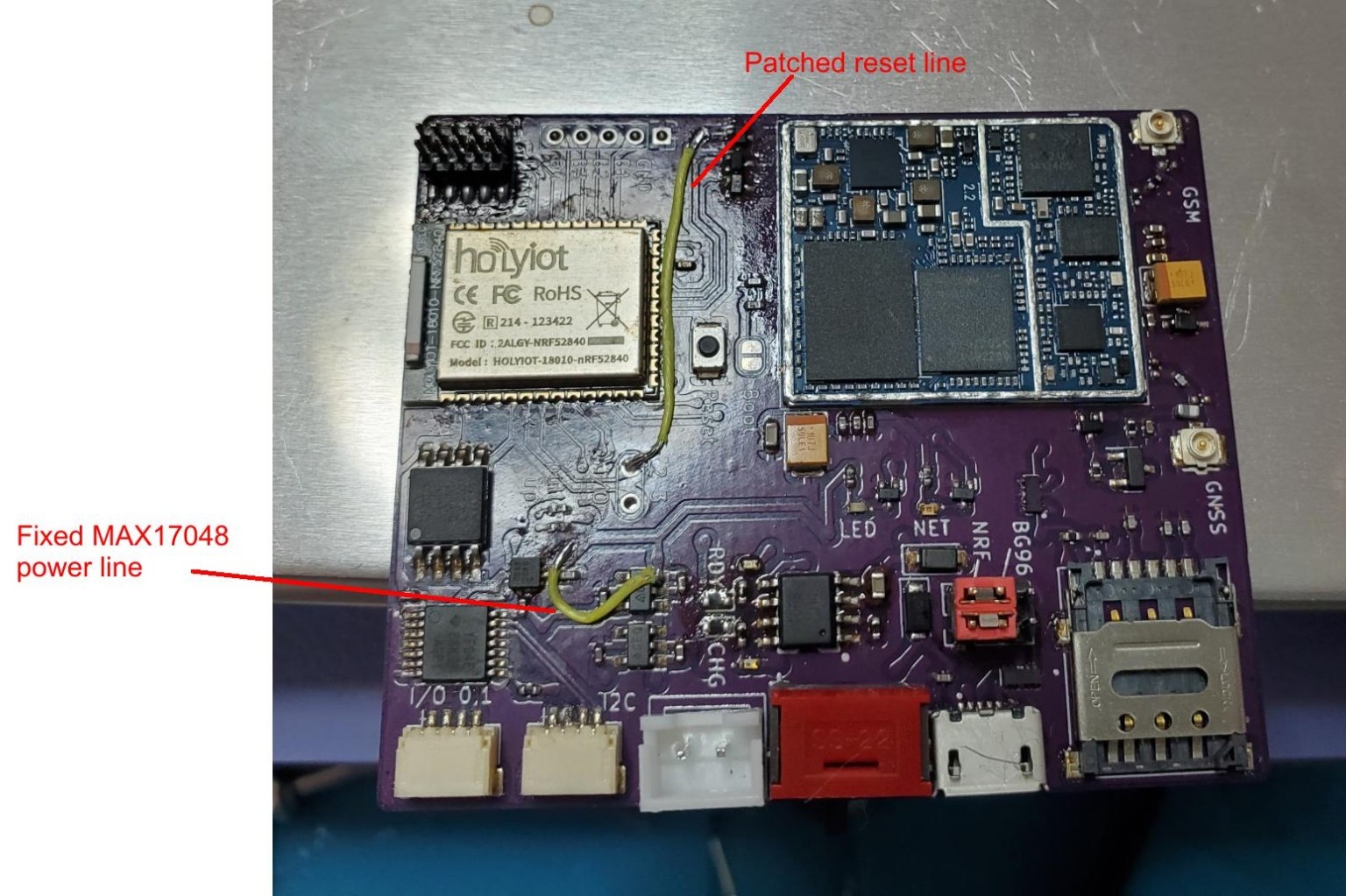
I got the display working then, reading the documentation for the MAX chip, figured out I'd got the power wiring wrong, so applied a patch to the board, and that "just worked".
 |
| Working board with screen after fix and patch |
After a lot of testing and reading, and firmware kicking, I had a theory that the problem was the reset line, I'd used a non-standard I/O port assuming/thinking from the documentation that that should work on any IO.... but on re-reading the NRF52840 spec carefully, it stated that IO18 was hardwired to be the reset line.
Oh fudge. So I cut the trace on the board, applied another patch wire, and now it seemed indeed to power up and worked reliably.
I tried re soldering the BG96, but it seemed that the multiple resolder cycles had killed it and I haven't got another. But otherwise the board is working and I can program it, albeit missing the somewhat crucial GPS and GSM features that a tracker kind of needs.
 |
| Board with power and reset patch. |
Improvements and fixes
So. Time to design a board to fix the minor flaws and take time with the experience to make some improvements for the next version:
 |
| Render of the next version, with improvements noted. |
I spent a lot of time going over the design again, and making some more improvements to the layout and shielding, as mentioned this is a four layer board and there are a *lot* of connections to the BG96 and NRF cpu modules. Also some of the surface mount components are *TINY*!!
 |
| A picture showing all four trace layers |
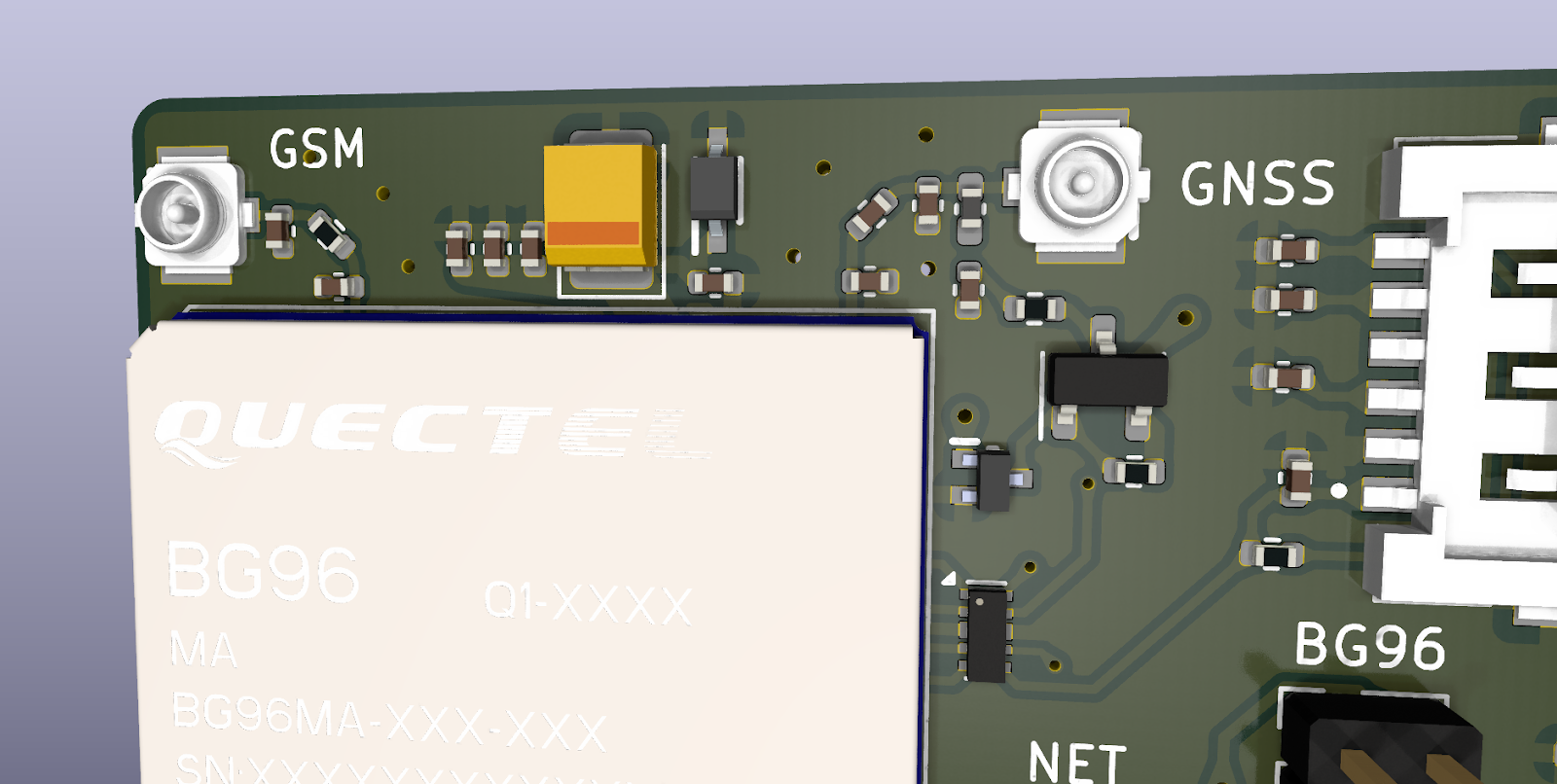
I'd read a bit about the antenna connections and tried redesigning the board to use straight connections, but wasn't happy that the board ended up 63mm high.... But also took the time to read how to design these traces and re-modelled them multiple times. This involved checking the calculations for trace width, distance to ground and thickness of the layers between the 4 layer layers.
 |
| Antenna design |
The documentation from Quectel (the BG96 GPS module manufacturer) is superb and has *lots* of detail explaining how to calculate these values along with tips for laying out the power lines and were screening is needed or needs to be omitted.
Many days later and I'm happy with the new design, in the end I decided to go back to curved traces which let me return to the more pleasing 50x60mm size! I've made lots of tiny improvements with this layout and ready to send off the designs for another board. I've also added lots of test-points.
Many days later and I'm happy with the new design, in the end I decided to go back to curved traces which let me return to the more pleasing 50x60mm size! I've made lots of tiny improvements with this layout and ready to send off the designs for another board. I've also added lots of test-points.
 |
| New design |
Up and running
In the meantime while I wait for new boards, I decided to get a BG95 module to test the slightly broken 'prototype' build to see if there were any other issues or areas to improve.... After a bit of hassle (some components were damaged during the repeated re-soldering to remove the BG96) I got a (cheaper) BG95 module soldered on, and spent some time fixing issues with the power-up signal (a transistor was dead) it powered up! Then the GPS didn't work, but narrowed that down to the board design wasn't big enough for the inductor I'd used so it hadn't soldered correctly (another improvement to make)...
 |
| Powered up and "blue light" - have a mobile signal. |
But it powered up! I'm absolutely astounded, this worked, this is such a complex build (for me), the next hassle was reworking some of my tracker code to work with the BG95 which is slightly incompatible, but a few hours later and we have a mobile signal! (ignore the "g" it's actually an LTE connection, but the BG95 returns a different string) and... (once the inductor was fixed) we have satellites (indoors even, the BG chips have amazing reception)
 |
| Running the current tracker code on the new build |
Using the existing tracker code, the screen is showing 6 satellites (indoors) a mobile signal, and it's picked up the ANT+ signal from the temperature sensor clipped to my bag, in another room. Clearly the battery logic needs tidying, I think it's confused because it's charging and connected to USB.
 |
| Running with a couple of random antenna I had |
 |
| Dumping the GPS data received |
I probably won't do too much more with this prototype build, I don't expect to actually use it, but I might take the time to make the code 'generic' for the two different modules, and use it to prototype a case.
Before ordering new boards and committing time and money to another build, I mainly wanted reassurance that my design actually functioned and I hadn't missed anything obvious, it's highlighted a few tiny errors and improvements, but thankfully (amazingly) there was nothing major wrong with the design or build. The power lines all work - the board uses 1.8v, 3.3v, 5v and 'battery' volt, the USB connection works, the charging works, the processor can wake up the GSM module and ask for data, the state signals all work and the antennas receive both mobile and GPS signals.
I'm absolutely delighted with this.
In the meantime, I've updated the PCB (again), and redesigned the charger circuit which I wasn't happy about I also decided I'd add a temperature/humidity sensor back on the board just because.
Since this write-up is getting a little long the overview of the latest version is on a new page.

